
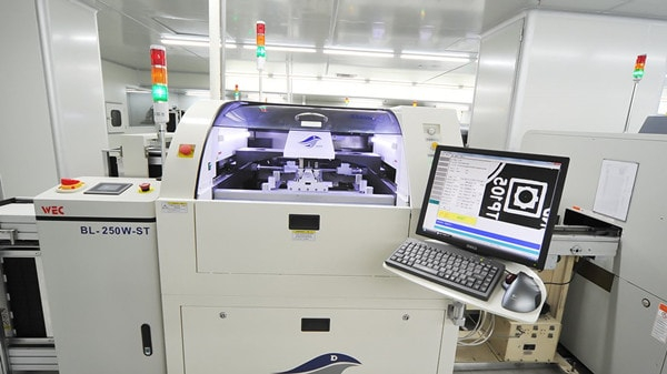
Friends who know hard brushed circuit boards should know that as the number of layers of the board increases, its manufacturing difficulty increases exponentially. Many people use the number of layers to manufacture the board to measure a company’s pcb manufacturing capability. Next, FS Tech Turnkey PCB Assembly Company will tell you the manufacturing process of four-layer pcb in the form of text.
Chemical Cleaning
PCB outer board cleaning: In order to draw a beautiful pattern on the PCB board, it is necessary to ensure that the anti-corrosion layer is firmly combined with the surface of the substrate, and the surface of the substrate is required to be free of oxides, oil, dust, fingerprints and other dirt. Therefore, before applying the anti-corrosion layer, the surface of the pcb sheet should be cleaned so that the surface of the copper foil should reach a certain degree of roughness.

Printed circuit board inner board cleaning: FS Technology must make the inner layers (second and third layers) before starting to make four-layer boards. The inner plate is a copper plate composed of fiberglass and epoxy resin matrix.
Cut and Laminate
Apply photoresist: In order to form the shape we need on the inner board of the pcb, FSPCB first pastes a layer of dry film (photoresist, photoresist) on the inner board. The dry film consists of polyester film, photoresist film and polyethylene protective film. When sticking the film, first peel the polyethylene protective film from the dry film, and then stick the dry film on the copper surface under the conditions of heat and pressure.
Exposure and Development
PCB Exposure: Under UV light irradiation, the photoinitiator absorbs light energy and decomposes it into free radicals. The free radicals then induce a polymeric crosslinking reaction in the photoluminescent polymerizable monomer. After the reaction, a polymer structure that is insoluble in dilute alkaline solution is formed. The polymerization reaction will continue for some time. To ensure process stability, do not peel off the Mylar film immediately after exposure, but leave it on for more than 15 minutes. The polymerization reaction will then continue. Peel off the polyester film before developing.
Printed circuit board development: The active groups in the unexposed part of the photosensitive film react with the dilute alkali solution to form a soluble substance, and after dissolving, the cross-linked and cured photosensitive pattern part is left.
Etching
During the production process of flexible printed boards or printed boards, unwanted copper foil is removed by chemical reaction to form the desired four-layer circuit board pattern, and the copper under the photoresist is not affected by etching.
Film removal, post-etching punching, AOI inspection, oxidation
The purpose of FSPCBA to remove the film of the pcb is to remove the resist layer remaining on the surface of the board after etching, exposing the underlying copper foil. Properly handle “membrane residue” filtration and waste liquid recycling. If the water wash after membrane removal can be completely cleaned, acid wash is not considered. The pcb board surface should be completely dry after cleaning to avoid moisture residue.
Laminate Protective Film
Before entering the press, the raw material of each multilayer circuit board should be prepared for the lay-up operation. In addition to the oxidized inner layer, a protective film (prepreg) is also required – epoxy impregnated fiberglass. The function of lamination is to stack sheets covered with protective film in a certain order and place them between two layers of steel sheets.
Lamination – Copper Foil and Vacuum Lamination
Copper Foil – Cover both sides of the current inner board with a layer of copper foil, then apply multiple layers of pressurization (extrusion that requires measurement of temperature and pressure over a fixed period of time) and cool to room temperature. The rest are multi-layer boards.
CNC drilling
Follow this mode for CNC drilling with precise inner layers. High drilling accuracy is required to ensure the holes are in the correct positions.
Plating – Through Hole
In order for the via to conduct between layers (metallizing the resin and fiberglass bundles in the non-conductive portion of the hole wall), the hole must be filled with copper. The first step is to deposit a thin layer of copper in the hole. The process is entirely a chemical reaction. The final copper plating thickness is 50 millionths of an inch.
Pre-hardening exposure and development on solder resist
The solder mask is used to expose the pads, the green oil layer, and actually dig holes in the green oil layer to expose the pads and other places that don’t need green oil coverage. Proper cleaning results in proper surface characteristics.
Surface Treatment
After completing all the above steps, FS Tech will do surface treatment to the four-layer circuit board. The process of hot air leveling solder coating Hal (commonly known as tin spraying) is to first dip the printed board in flux, then dip it in molten solder, pass between two air knives, and blow the printed board with hot compressed air in the air knife. Remove excess solder from the board and drain the excess solder into the metal holes.
Goldfinger (or edgeconnector) is designed to use the connector connector as an outlet for connections outside the board. Therefore, it requires a gold finger manufacturing process. Gold was chosen for its superior electrical conductivity and resistance to oxidation. However, due to its high cost, it is only used for gold fingers, local electroplating or electroless gold plating.
The above is the whole process of making a four-layer PCB board by FSPCBA, I hope it can help all those in need
You can see more content about pcb knowledge in FS Technology PCB blog.


